Wednesday, May 15, 2013

Difference between 2G and 3G Technology

Difference between 2G and 3G Technology


Second Generation (2G) technology was launched in the year 1991 in Finland. It is based on the technology known as global system for mobile communication or in short we can say GSM. This technology enabled various networks to provide services like text messages, picture messages and MMS. In this technology all text messages are digitally encrypted due to which only the intended receiver receives message. These digital signals consume less battery power, so it helps in saving the battery of mobiles.
 
The technologies used in 2G are either TDMA (Time Division Multiple Access) which divides signal into different time slots or CDMA (Code Division Multiple Access) which allocates a special code to each user so as to communicate over a multiplex physical channel.
 
3G technology generally refers to the standard of accessibility and speed of mobile devices. It was first used in Japan in the year 2001. The standards of the technology were set by the International Telecommunication Union (ITU). This technology enables use of various services like GPS (Global Positioning System), mobile television and video conferencing. It not only enables them to be used worldwide, but also provides with better bandwidth and increased speed.
 
This technology is much more flexible as it can support 5 major radio technologies that operate under CDMA, TDMA and FDMA. CDMA accounts for IMT-DS (direct speed), IMT-MC (multi carrier). TDMA holds for IMT-TC (time code), IMT-SC (single carrier). This technology is also comfortable to work with 2G technologies. The main aim of this technology is to allow much better coverage and growth with minimum investment.
 
2G vs 3G Technology
Figure: Evolution of Mobile system from 2G to 3G
 
 
Difference between 2G and 3G Technology
·         Cost: The license fee to be paid for 3G network is much higher as compared to 2G networks. The network construction and maintenance of 3G is much costlier than 2G networks. Also from the customers point of view the expenditure for 3G network will be excessively high if they make use of the various applications of 3G. 
 
·         Data Transmission:  The main difference between 2G and 3G networks is seen by the mobile users who download data and browse the Internet on the mobile phones. They find much faster download speeds, faster access to the data and applications in 3G networks as compared to 2G networks. 2G networks are less compatible with the functions of smart phone. The speed of data transmission in 2G network is less than 50,000 bits per sec while in 3G it can be more than 4 million bits per sec.
 
·         Function: The main function of 2G technology is the transmission of information via voice signals while that of 3G technologies is data transfer via video conferencing, MMS etc.
 
·         Features: The features like mobile TV, video transfers and GPS systems are the additional features of 3G technology that are not available with 2G technologies.
 
·         Frequencies: 2G technology uses a broad range of frequencies in both upper and lower bands, under which the transmission depends on conditions such as weather. A drawback of 3G is that it is simply not available in certain regions.
 
·         Implication: 3G technology offers a high level of security as compared to 2G technology because 3G networks permit validation measures when communicating with other devices. 
 
·         Making Calls: Calls can be made easily on both 2G and 3G networks with no real noticeable differences except that in 3G network video calls can also be made. The transmission of text messages and photos is available in both the networks but 2G networks have data limit and the speed of the data transmission is also very slow as compared to 3G.
 
·         Speed:  The downloading and uploading speeds available in 2G technologies are up to 236 Kbps. While in 3G technology the downloading and uploading speeds are up to 21 Mbps and 5.7 Mbps respectively.

How Scientific Calculator works

How Scientific Calculator works


Scientific calculators are more of a habit for any engineer. Loaded with features that can solve complicated trigonometric, logarithmic and exponential equations in just a blink of eye, scientific calculators are nothing less than a pocket sized brain. Let’s find out what makes this small sized gadget tick.
 
Scientific-Calculator.jpg
 
Most of the scientific calculators, irrespective of the manufacturer, come in a hard plastic casing as shown above.  The layout of the buttons is neat and ergonomic so that calculators can be used for long time without posing any risk of strain to the wrist and also ensuring correct key stroke each time, irrespective of the finger size pressing them.
PCB
 
PCB-1.jpg
 
A plastic casing houses the PCB, batteries and the LCD display of the calculator. A double sided PCB is used in a scientific calculator. While one side has the COB IC, the necessary circuitry and connections to the LCD, the other side forms the keypad which contains the tracks that generate signals corresponding to the keys pressed. The rear side of the PCB is shown below.
 
PCB-2.jpg

Processing Core: COB IC or no COB?
 
Processing-Core-1.jpg
 
Using a COB IC is a cost effective feature as it saves significant amount of hardware and carries out all the functions of the calculator but usually takes away the capability of the calculator to be user programmable. This also spells the difference between an ordinary, off the mill pocket calculator used for simple addition and multiplication purposes, and a sophisticated scientific calculator capable of diverse computation. COB ICs are mainly used in those calculators which are non-Programmable while programmable calculators do feature a separate Packaged or Surface mounted microprocessor based IC which are interfaced with external flash memory.
 
Programmable calculators can be instructed to store user defined data and formulas.  The chip would not be visible explicitly in scientific calculators too as that too would look like a COB IC owing to the fact that the chip is covered with a layer of epoxy. A few suitable ICs that have been used in programmable calculators are the 8502 Microprocessor which has been used in HP 35s series of scientific calculators and the ARMv4T chips used in much more powerful calculators which offer graph plotting functionality and support for external memory inputs like memory cards.
Keypad
 
Keypad-1.jpg
 
Shown in the image above is the rear side of the plastic keypad and the PCB. Patterns are drawn on the PCB surface that generate the signal to the corresponding key that is pressed and convey in to the COB IC. The keypad works in the same way as keyboard does. The plastic switches that appear on the casing are connected to a rubber keypad. When the key is pressed, the black rubber mark under the rubber keypad touches the PCB and completes the track for signal transmission.
LCD Display
 
LCD-Display.jpg
 
As per the features provided in the calculator, LCD screens of the calculator can be of various sizes and type. While a simple calculator has a 16X2 LCD display, the ones enabled with advanced features have a LCD dot matrix display too. High end scientific calculators even have a colourful display.
 
Shown in the image above is a two line display LCD. Top line is a LCD dot matrix display while the lower part is LCD display using seven segment digits. The LCD is connected to the PCB with the aid of heat seal connector. A heat seal is a light connector made out of polyester film. Two layers of polyester films are adhered (sealed) togetherat high temperature, using a conductive paste, thus the name heat seal.
BATTERY
 
BATTERY.jpg
 
The type of batteries used depends on the calculator’s features. More the features or bigger the LCD display, more powerful the battery should be. Shown above is an AA pencil cell combination that gives power to the calculator. Button cell or “AAA” batteries are also used in many calculators. Average life of such a battery pack is 1-2 years (though it varies with each battery type and from calculator to calculator). Adding a solar panel enhances the battery life so that the reason for replacing the calculator is not the dying out of the batteries, but something else like physical damage due to dropping it from a height. Moreover, calculators run on very low power and do not run dry that easily.  In order to consume least possible battery power, calculators have an Auto Power Off feature. This feature is managed by “Power Control Consumption System” which switches the calculator off when no key is pressed for certain duration. Usually this time is 7-9 minutes and if calculator is in middle of any calculation (which usually does not happen), it saves the data for ease of the user.

The first scientific calculator was released in late 1960s by Hewlett Packard and numerous electronic manufacturers followed suit. Initially expensive and feature restricted, engineers have continually crammed more and more features into that little space as the semiconductor manufacturing industry continues to mature.


Tuesday, May 14, 2013

DC Motor Interfacing With Micrcontroller

DC Motor Interfacing With Micrcontroller

DC Motors are small, inexpensive and powerful motors used widely in robotics for their small size and high energy out. A typical DC motor operates at speeds that are far too high speed to be useful, and torque that are far too low. Gear reduction is the standard method by which a motor is made useful .Gear’s reduce the speed of motor and increases the torque.
Choosing a DC Motor Depends on application.Prefer following:
  • DCMotor with Gear head
  • Operating voltage 12V
  • Speed


  •  


Drive basics of DC Motor

Red wire Black wire Direction of rotation
Positive Negative Clock wise
Negative Positive Anti clock wise
Logic Logic Direction
1 0 Clock
0 1 Anti clock
Direction Pulse to
Clock wise A and C
Anti Clock wise B and D

Bi-Direction control of DC Motor

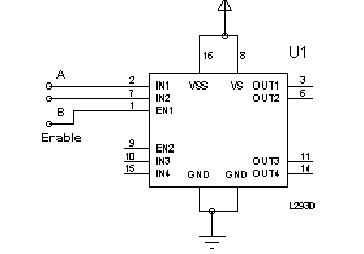
H-Bridge Circuit using transistors for bidirectional driving of DC motor. H-Bridges in IC’s to reduce the drive circuit complexity . L293D is a dual H-Bridge motor driver, So with one IC we can interface two DC motors which can be controlled in both clockwise and counter clockwise direction and if you have motor with fix direction of motion the you can make use of all the four I/Os to connect up to four DC motors. L293D has output current of 600mA and peak output current of 1.2A per channel. Moreover for protection of circuit from back EMF ouput diodes are included within the IC. The output supply (VCC2) has a wide range from 4.5V to 36V, which has made L293D a best choice for DC motor driver.
As you can see in the circuit, three pins are needed for interfacing a DC motor (A, B, Enable). If you want the o/p to be enabled completely then you can connect Enable to VCC and only 2 pins needed from controller to make the motor work.
**To Move the motor Clockwise And Anticlockwise,Must be use two separate Power source,one for microcontroller and another for driving motor with Driver IC.
Here,i have used ATMEGA32 micrcontroller and  Code is written in C  using AVR Studio 5.0.

Source Code

/*
* DCMotorControl.c
*
* Created: 4/1/2011 12:08:10 AM
*  Author: sfg
*/
#include <avr/io.h>
#include <util/delay.h>
int main(void)
{
DDRD=0xFF; //PORTD declared as output
PORTD=0×00;
DDRB=0×00; //PORTB as input
while(1)
{
//Pin 0 of PORTB high,then Moves Clockwise
//A–1–PD0
//B–0–PD1
//Enable–1–PD2
if(PINB==0×01)
{
PORTD=0×05;
//_delay_ms(5000);
}
//Pin 0 of PORTB Low,then Moves AntiClockwise
//A–0–PD0
//B–1–PD1
//Enable–1–PD2
else
{
PORTD=0×06;
//_delay_ms(5000);
}
}
}

http://vshamu.files.wordpress.com/2011/04/dcmotorcontrol.jpg

Led blinking program with 8051 Microcontroller and Keil uVision4

Led blinking program with 8051 Microcontroller and Keil uVision4

The first “Hello World!” project I prefer for Microcontroller is LED Blinking. I have used ATMEL’s 89C51 (40-pins DIP) 8051 architecture microcontroller which is ideal for first time learning MCU Chip.  The program is very simple and straight forward, that uses a delay procedure  loop based software delay.

Source Code

Here,i have  written code  in C using Keil uVision4.
#include <REGX51.H>
void msdelay(unsigned int );
void main(){
P2=0×00;  //all pin of PORT2 declared as output
//infinite loop
while(1){
P2=0xFF;   //all pin high
msdelay(250);    //delay
P2=0×00;   //all pin low
msdelay(250); //delay
}
}
//delay function
void msdelay(unsigned int value){
unsigned int x,y;
for(x=0;x<value;x++)
for(y=0;y<1275;y++);
}
In C programs you cannot be sure of delay, cause  it depends on compiler how it optimize the loops as soon as you make changes in the options the delay changes.
you will have to use Timers for making exact delays….. it does not matters whether u need delays of ms , us or even seconds…
below is a function of 1 second using timers…..
// the idea is to make a 50ms delay and run it 20 times as 20x50ms= 1000ms= 1sec
delay_1s() // timer of 1 sec
{
int d;
for(d=0;d<=20;d++)
{
TMOD=0×01;
TL0=0xFD;
TH0=0x04B;
TR0=1; // start timer.
while(TF0==0); // run until TF turns to 1
TR0=0; // stop timer
TF0=0; // reset the flag
}
}

http://vshamu.files.wordpress.com/2011/03/s.jpg

Servo Motor

Servo Motor
 
 
Servo Motors are DC Motors (check out how DC motor works) with a servo mechanism to provide a precise angular motion. Pulse width modulation (PWM) technique is used to set the angle of rotation. Generally RC servo motors have a rotation limit of 900 to 1800 but servos with high rotation angles are also available.
 
DC Servo Motor
A Servo motor with a rotation limit of 1800 is shown in the image.
 
Servo Motor Wiring 
Servo Motor Feedback Circuit
The circuit shown in the above image consists of the necessary control and feedback providing components.
Servo Motor ARM
A servo horn or also known as servo arm which rotates with the motor spindle.
Servo Motor Gear Assembly
Gears arrangement plays an important role to provide necessary high torque and to provide feedback.
Servo Motor Gears
The above image shows various gears used in a servo motor.
Motor and Potentiometer in Servo motor
The above image shows the DC motor and the potentiometer which is used to provide feedback to the electronic circuitry. It is connected with the DC motor with the help of gear assembly. As soon as the motor starts rotating the potentiometer also starts rotating and the output of potentiometer i.e. voltage across the middle terminal changes which acts as the feedback signal to indicate the degree of rotation of the motor.


Potentiometer Working

Potentiometer Working
 
Potentiometer also known as pot is generally used in circuits to provide variable resistance or variable voltage. The heart of the potentiometer is a resistive strip inside it through which one can adjust the amount of resistance/voltage to pass in a circuit through it. Potentiometers are commonly used in circuits for various purposes like to control volume in audio circuits, to regulate the speed of the motor in a fan, as light dimmer, etc.
A potentiometer is shown in the images below.

Potentiometer, pot or variable resistor  
 
Potentiometer
Potentiometer, pot or variable resistor2 
You can see there are three terminals on the potentiometer which are used to connect it to any external circuit.
Terminals of a potentiometer
 
The metal cap in the above image forms the outer covering and encloses all parts of the potentiometer.

Metal bearing of potentiometer 
The metal bearing shown in the left side of the above image is used for mechanical connections.
Resistive Strip of potentiometer
Resistance Strip in potentiometer or variable resistor
  
You can see two concentric circles in the image above. The outer black arc (resistive strip) on the plate is the heart of the potentiometer. It is used to provide variable resistance to the circuit. The inner circle made up of a conductive material is connected to the middle terminal.
Conductive Brushes of Potentiometer
  
As shown in the figure, the brush, generally made up of stainless steel has two sections of dents. First one with three dents moves on the resistive strip and second one with two dents moves on the inner circle which is connected to the middle terminal (wiper).
The brush is attached to the shaft. It moves on the plate and the resistance applied to the circuit, depends on the position of the brush on the plate.
Variable resistance Strip in potentiometer
  
When we rotate the external shaft, the position of the brush varies accordingly. The resistance applied in a circuit depends on the position of the brush. The brush is designed so as to connect the resistive strip to the middle terminal via inner conductive circular metal plate which in turn is connected to the middle terminal of potentiometer at every instant.


Monday, May 13, 2013

Working of XLR Connector

Working of XLR Connector

Every year, technology sector companies invest millions of dollars in R&D to improve their products and release new products. An important part of these products is characterized by the connectors they use. For instance, a computer requires USB and PS2 Connector, a headphone requires TRS connector and a telephone requires RJ11 connector and so on. For high quality professional sounds, XLR connector is widely preferred. The term XLR derives its name from Cannon “X” series (where it was first used). Terms “L” and “R” are derived from latch and rubber used in the connector.
From a good microphone to a tuned guitar, all gadgets should be well matched up to the needs of the performer. Playing a critical role in professional audio applications is an XLR connector. Connecting the microphone to the amplifier, these connectors form an indispensible part of any electric instrument.
A 3 pin connector specifically designed for audio applications, XLR are known to be used in almost every wired microphone. Let’s get into the internal structure of the connector and discover various parts that make the connector function.
XLR-1.jpg 
Front Structure: The image above shows front view of a 3 pin XLR connector. The connector is made up of alloy (usually of zinc) and plastic.
There are three pins to take the input from the microphone. A small steel latch locks the microphone with the connector.
XLR-2.jpg
Input Pins: The inputs are labeled from 1 to 3 which aids in identifying the right pins when the wiring of the connector is done. In a professional sound system, inputs 1, 2 and 3 get the following wire combination:
·                     Input 1 for Ground
·                     Input 2 for Live
·                     Input 3 for Negative
XLR-3.jpg 
Locking the device  : It is very essential for any connector to connect tightly to its corresponding device. A latch based locking mechanism solves this purpose in a microphone.
The larger latch is accessible to the user while the smaller one hides under the device. A rubber ring protects the device from wear and tear.
In order to disconnect the device, the larger latch is pressed which in turn presses the smaller latch. The device can be then removed from the XLR connector.
XLR-4.jpg
Rear View: The rear side of the connector is the output part from which the wire extends out. The blue colored plastic casing helps in griping the connector to connect or disconnect. The black rubber casing which is called the sleeve keeps the wire straight thereby  avoiding any mechanical damage to the connections.
XLR-5.jpg
The image above shows the connection of the plastic casing with the alloy structure.
XLR-6.jpg 
Wire Streamliner: When separated, the alloy region has an inverted bullet like plastic coming out of its bottom. This part streamlines the wires inserted to connect to the pins of the connector.
XLR-7.jpg
Interface for Wires: The image above shows the pins of the connector where the wires are soldered.
XLR-8.jpg

Lever for Latch movement:  The latches placed on the connector for holding the device have a vertical back and forth movement because of a lever placed beneath them. This lever structure gets pressed whenever the device has to be disconnected and as soon as force gets off, it places the latches back in their rest state. Thus, having a spring like motion to assist latch movement is the prime function of the lever.
XLR-9.jpg
Holding the input pins: The image above shows a small section through which the pins of the connector are held. The input pins are firmly held in the plastic mould which restrict their movement. The pins also have certain extensions that limit their movement beyond a certain limit.

XLR-10.jpg

The connecting pins have a structure similar to a flute. An extension which restricts the movement inside plastic molding can be seen in the image above.